
Open instruction set architectures (ISA) offer the promise of enabling a number of key benefits to designers charged with delivering next generation embedded products. In addition to providing a lower-cost alternative to proprietary microprocessors, open ISAs can readily be customized by adding additional instructions, enabling better support for specific application requirements in areas such as vision processing or security, for example.
The RISC-V Foundation was formed as a non-profit consortium to commercialize the University of Berkeley’s RISC-V ISA. The RISC-V Foundation is responsible for maintaining the core instruction set specification and associated licensing. In addition, a range of software tools are available including compilers, debuggers, and verification suites.
In order to bring the benefits of open ISA to its worldwide customer base, ASTC has developed in-house implementations of RISC-V. These cores are available either as an option in the ASTC Intelligent Sensor and Power (ISP) Platform for rapid ASIC derivative design or as standalone IP blocks.
RV32EC_P2 Processor Core IP
ASTC’s RV32EC_P2 IP is a 2-stage pipeline RISC-V processor core, designed to meet the needs of small, low-power embedded applications, running only trusted firmware.
RISC-V RV32EC_P2 CORE: BLOCK DIAGRAM
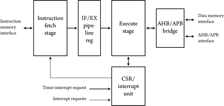
The RV32EC_P2 processor core can be used in both ASIC- and FPGA-based design flows, and offers the following features:
- RISC-V RV32E base instruction set, compliant with RISC-V User-Level ISA Version 2.2.
- RVC standard 16-bit compressed instructions for common RV32 instructions, for reduced code size.
- Optional “M” standard extension for integer multiplication and division instructions.
- Optional inclusion of full RV32I register set (32 registers).
- Provision for application-specific instruction set extensions, e.g. for DSP operations.
- Simple machine-mode privileged architecture with direct physical addressing of memory, compliant with RISC-V Privileged Architecture Version 1.10.
- 20 extended interrupts, plus timer and software interrupts.
- Provision for external interrupt controller for additional interrupt sources.
- All interrupts and exceptions vectored for fast interrupt response.
- Wait-for-interrupt instruction supports clock gating for low-power idle state.
- 2-stage pipeline comprising fetch and execute stages. Most instructions complete in one clock cycle.
- Tightly-coupled memory interfaces for ASIC ROM and SRAM memories or FPGA block memories.
- AHB-Lite or APB interface for extended memory and memory-mapped I/O.
- GNU tool chain and Eclipse development environment for firmware development.
- Firmware and virtual prototype development supported by ASTC’s VLAB system-level design tools.
- Accompanying machine-mode timers (AHB and APB versions) operating in processor clock domain or separate always-on timer clock domain.
- Accompanying platform-level interrupt controller (PLIC) for up to 1023 interrupt sources.
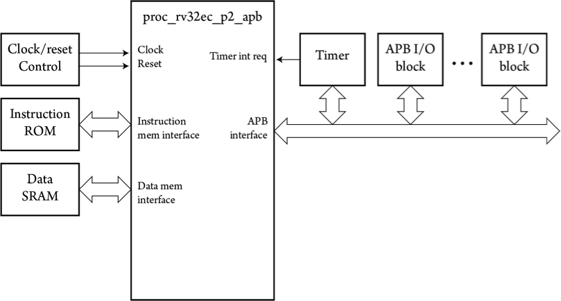
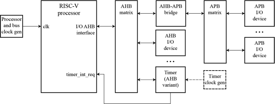
The processor interfaces to separate compiled memory blocks for code and data memories, and to memory mapped I/O blocks connected to Advanced High-Performance Bus (AHB) and Advanced Peripheral Bus (APB) buses. A clock control block gates clocks to the core depending on the operating mode.
RISC-V RV32EC_P2 CORE: APPLICATION DIAGRAM WITH AHB INTERFACE

For simpler systems, a variant of the processor core provides just an APB interface for I/O devices. Other aspects are the same as for the variant with AHB interface.
RISC-V RV32EC_P2 CORE: APPLICATION DIAGRAM WITH APB INTERFACE
RV32IC_P5 Processor Core IP
ASTC’s RV32IC_P5 IP is a larger, 5-stage pipeline core RISC-V processor, designed to meet the needs of medium-scale embedded applications that require higher performance, cache memories, and running a mix of trusted firmware and user application code.
RISC-V RV32IC_P5 CORE: BLOCK DIAGRAM
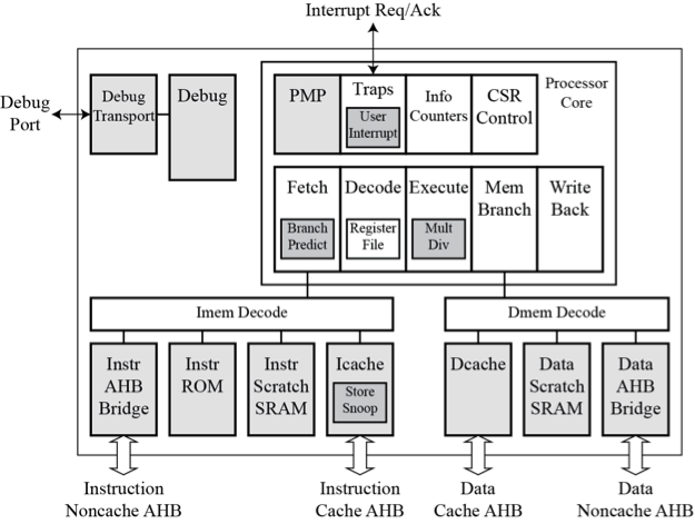
It can be used in both ASIC- and FPGA-based design flows, and offers the following features:
- RISC-V RV32I base instruction set, compliant with RISC-V User-Level ISA Version 2.2.
- RISC-V “A” standard extension instructions for critical sections in a uniprocessor system.
- RVC standard 16-bit compressed instructions for common RV32 instructions, for reduced code size.
- Machine-mode and user-mode privileged architecture with direct physical addressing of memory, compliant with RISC-V Privileged Architecture Version 1.10.
- Optional standard physical memory protection (PMP) with configurable number of entries, to support protected execution of application code.
- Optional “N” standard extension for user-mode exception and interrupt handling.
- Optional “M” standard extension for integer multiplication and division instructions.
- Provision for application-specific instruction set extensions, e.g. for DSP operations.
- 20 extended interrupts, plus timer and software interrupts.
- Provision for external interrupt controller for additional interrupt sources.
- All interrupts and exceptions, including those delegated to user mode, may be vectored for fast interrupt response.
- Wait-for-interrupt instruction supports clock gating for low-power idle state.
- 5-stage pipeline comprising fetch, decode, execute, memory access, and write back stages.
- Optional branch prediction, branch target buffer, and return address stack, with configurable sizes and associativity, for reduced branch latency.
- Tightly-coupled scratchpad memory interfaces for ASIC ROM and SRAM memories or FPGA block memories.
- Optional instruction and write-back data cache memories with configurable line sizes, number of sets, and associativity.
- AHB-Lite interfaces for extended memory and memory-mapped I/O.
- GNU tool chain and Eclipse development environment for firmware development.
- Firmware and virtual prototype development supported by ASTC’s VLAB system-level design tools.
- Accompanying machine-mode timers (AHB and APB versions) operating in processor clock domain or separate always-on timer clock domain.
- Accompanying platform-level interrupt controller (PLIC) for up to 1023 interrupt sources and separate machine-mode and user-mode targets.
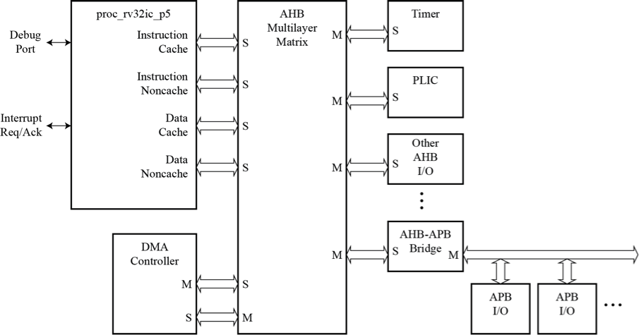
The processor core interfaces to separate compiled memory blocks for code and data memories, and to memory-mapped I/O blocks connected to AHB and APB buses. The application diagram shows that the processor AHB buses connect as masters to an AHB multilayer matrix, along with a DMA controller master. Slaves on the bus matrix include a RISC-V timer, a RISC-V PLIC, and a bridge to an APB bus for smaller I/O controllers.
RISC-V RV32IC_P5 CORE: APPLICATION DIAGRAM
RISC-V Timer IP
ASTC’s RISC-V Timer IP comprises a suite of timers, each conforming to the RISC-V standard machine timer specification.
For simple applications in which the timer counts processor-clock cycles, variants are provided without clock-domain crossing (CDC). Alternatively, for low-power applications in which the system clock may be gated-off or disabled, ASTC also offers a variant with CDC counts of cycles of a low-frequency always-on clock (e.g., a clock provided by a low-power 32kHz oscillator).
Variants of the timer with AHB bus interfaces allow for use in systems with complex bus structures. Alternatively, variants with APB bus interfaces allow for use in small systems with simple APB-only bus structures.
RISC-V TIMERS: APPLICATION DIAGRAM WITH AHB INTERFACE
RISC-V TIMERS: APPLICATION DIAGRAM WITH APB INTERFACE
RISC-V Platform-Level Interrupt Controller (PLIC) IP
ASTC’s RISC-V PLIC IP is a platform-level interrupt controller conforming to the RISC-V PLIC specification, for use in systems with a large number of interrupt sources and multiple processor targets for interrupt delivery. It is configurable, and can be tailored to the number of sources and targets required by an application. The IP offers the following features:
- Configurable number of interrupt sources, from 31 to 1023.
- Configurable number of target hart contexts, from 1 to 32.
- Configurable number of priority levels, from 1 to 255.
- Each interrupt source configurable for synchronous or asynchronous request signals, level sensitivity, or rising/falling/both edge sensitivity.
- AHB-Lite interface for register access for setting priorities, interrupt enables, and claiming/completing interrupts.
- Protection for secure control of interrupt allocation to targets.
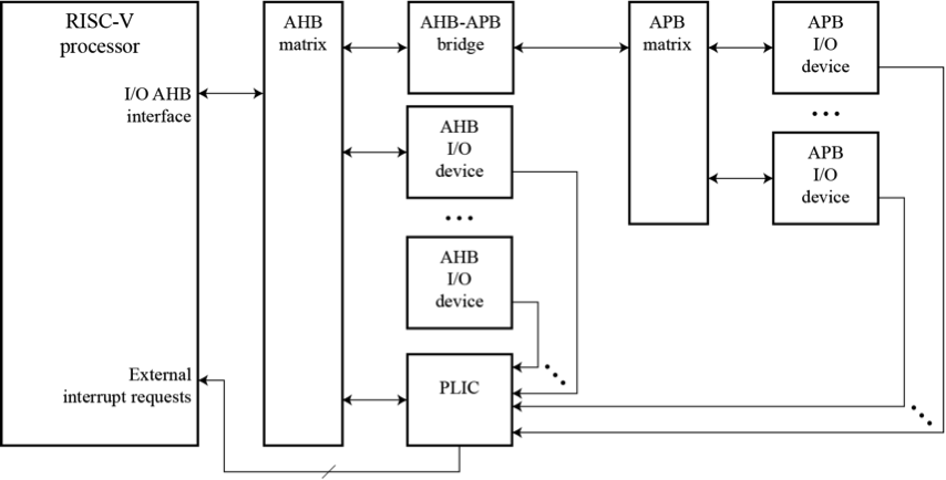
In a single-processor application, the PLIC connects to the AHB bus matrix and collects interrupt requests for AHB and APB I/O devices. The PLIC target interrupt requests connect to the RISC-V processor’s external interrupt request inputs, providing interrupts for machine-mode and user-mode contexts.
RISC-V PLIC: SINGLE PROCESSOR APPLICATION DIAGRAM
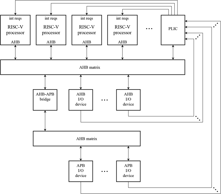
In a larger multiprocessor application, the PLIC connects to the shared AHB bus matrix and collects interrupt requests for AHB and APB I/O devices. The PLIC treats each execution context (machine mode, supervisor mode, user mode) on each processor as a separate target for interrupts. An interrupt can be enabled for multiple targets. The first processor to claim the interrupt by reading the corresponding PLIC claim register is responsible for handling the interrupt and for indication completion to the PLIC.
RISC-V PLIC: MULTIPROCESSOR APPLICATION DIAGRAM
For all IP blocks, ASTC provides the following deliverables in support of customer application needs, and can also supply a range of additional supporting IP blocks:
| Deliverables: | Related IP: |
| Synthesizable Verilog RTL | SPI master and SPI slave controllers |
| Sample synthesis script for trial synthesis | I2C master and I2C & I3C slave controllers |
| Detailed data sheet and integration guide | UART controller |
| Reference designs | General purpose I/O (GPIO) controller |
| Optional product/project support services | Watchdog and sleep timers |
For more information on ASTC’s unique range of products and services supporting RISC-V product development, please contact us.