
Fast Functional Verification of Mixed Analog and Digital SoCs: Application Brief
IC Engineering: Wireless
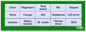
For mobile handsets/ wireless, ASTC verified power management ICs (PMICs) and RF ICs.
Program included:
- SystemVerilog testbench
- Auto-generation of artifacts
- Functional coverage point analysis and measurement
- Execution of actual software drivers exercising RTL pre-silicon
- Development of abstracted power management models for high-level system simulation
ASTC also did design of digital control for a complex buck regulator.
IC Engineering: FPGA Prototyping for Mobile
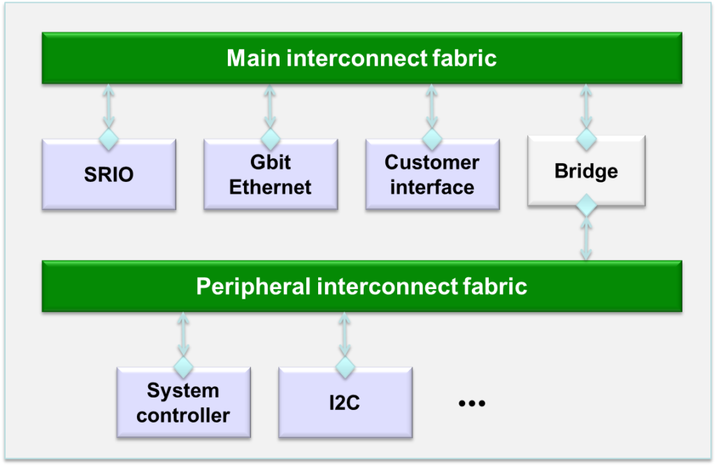
Wireless communications infrastructure and Ethernet chips,
ASTC delivered both design and verification of subsystems in wireless communications infrastructure chips, with Gigabit Ethernet. ASTC identified architectural and functional issues during verification and performed FPGA prototyping for the subsystems.
This communications company subsequently engaged ASTC for multiple projects.
IC Engineering: FPGA Verification
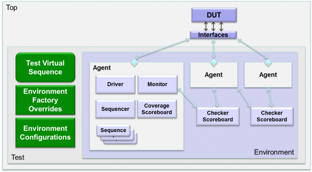
In verification of a new FPGA chip for a major vendor, ASTC reviewed verification plans, identified methodology gaps, and drove verification signoff. Verification included digital block level, OVM system level, AMS, and software, with full traceability from system specifications, to verification requirements, to test cases, to results.
ASTC verified 1G/10G Ethernet MACs, PCIe, SRIO, SPI, and configuration interface blocks and developed innovative techniques to accelerate full chip-level functional verification, abstracting programmable fabric to make simulation time-tractable.
Results? “This is the best silicon we have ever seen.”
IC Engineering: Turnkey ASIC Design in Consumer
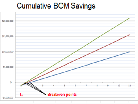
For an industry leader in consumer products, the business case for ASIC integration was clearly attractive:
- An initial investment of approximately $1M
- Breakeven within approximately 2 years
- ROI of 7x to 14X in 8 years
Also, other business and technical advantages contribute to competitive and market share wins:
- Performance
- Security and IP protection
- Power
- Higher yield and reliability
- Reduced inventory
- Lower packaging costs
- Lower cost of goods
- Eliminated or reduced need for redesigns due to component obsolescence
IC Engineering: Digital and Analog
Recent designs span analog and digital blocks.
- Very low jitter PLL from 40MHz up to 2 GHz output, from -20C to 125C temperature range
- 16 bit 1MHz sigma delta ADC.
- Communication blocks including SPI, I2C, DSI, PSI5.
And, integration of a wide range of SoCs across communications, automotive and networking.