One of the most visible shifts in the embedded world over the past decade has been the rapid rise of multi-sensor based applications, particularly in the low-power, mobile-device marketplace. In fact, strong year-on-year growth in sensor sales is being propelled by multiple industry trends, all playing out in parallel. Whether it’s the rapid expansion of IoT applications, widespread use of sensors across the automotive sector, or the inclusion of multiple devices in smartphones (itself accounting for sensor shipments in excess of 10 billion units annually), it’s clear that product designs now need to handle a broad range of sensing devices, both efficiently and with minimal complexity. This has led to a significant step forwards in standards supporting the necessary interfaces, one that brings product designers much greater freedom, allowing them to increase the number of sensors they can utilize, and to do so with higher bandwidths and lower power consumption.
The MIPI Alliance’s I3C interface is an evolutionary standard that improves upon the sensor management features of I²C, while maintaining backward compatibility, and is intended for use as a single interface that can support any sensor.
This new standard offers a flexible, multi-drop interface between the host processor and peripheral sensors, supporting the expanding number of sensors deployed in embedded systems. The main purposes of the I3C standard are threefold:
- Standardize sensor communication;
- Reduce the number of physical pins used in sensor system integration;
- Support low-power, high-speed, and other critical features that are currently covered by I²C and SPI.
The full MIPI I3C standard supports the integration of sensors as diverse as mechanical, biometric, or motion-based, whilst also embracing the more traditional approaches used in I²C, SPI, and UART. The standard focusses on unifying what had become a rather fragmented and often ad-hoc approach to sensor interfacing, and doing so in such a way as to minimize the physical resources required for its implementation.
To meet the fast-changing needs of its broad and diverse base of embedded customers and applications, ASTC was an early adopter of I3C, resulting in the development and productization of a comprehensive, MIPI-compliant I3C Slave block. This IP implements a low-power, fully featured slave interface supporting the following key protocols:
- I3C single data rate (SDR up to 12.5 Mbps)
- I²C standard mode (100 kbps)
- I²C fast mode (Fm, 400 kbps) and fast-mode plus (Fm+, 1 Mbps)
- I²C high-speed mode (3.4 Mbps)
ASTC’s I3C slave IP block has been architected both to streamline existing sensor-based product designs and to provide the maximum feature-set and flexibility in support of all future developments, particularly for power-constrained applications in markets such as mobile, IoT, and consumer. The feature set offered includes the following:
- I3C slaves can initiate in-band interrupts, something that would otherwise consume a dedicated signal line for both I²C and SPI devices. The in-band interrupt feature also enables slaves to issue a “start” signal when the bus is available (i.e. idle), thereby further reducing power consumption.
- In-band integrated commands (CCC) support.
- Multiple sensors can operate on the same communication bus, while eliminating the additional logic signals otherwise required to support interrupt or sleep mode functionality.
- Dynamic addressing.
- The I3C slave interface has improved power performance while providing greater than an order of magnitude improvement in speed over I²C.
- Backward compatibility with I²C.
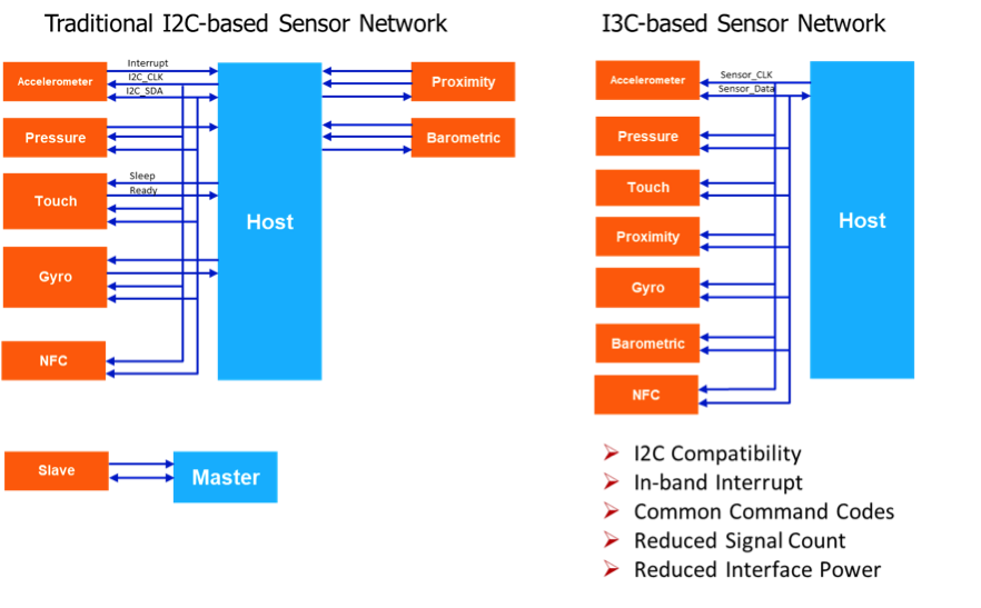
I3C NETWORK DIAGRAM
In collaboration with its customers, ASTC has a long history both of being closely involved with the development and delivery of a range of leading-edge, bi-directional two-wire serial communications interface IP implementations, including to I3C, I²C, SPI, PSI5, and DSI specifications. Our customer engagements span from architecture consulting and semiconductor design, through to complete turnkey design implementations, including application software. Markets served include mobile and consumer, automotive, medical, and on into IoT.
Along with amassing an extensive body of consulting and implementation experience, ASTC has built a comprehensive set of re-usable technology assets that can dramatically shorten time-to-market for the most challenging customer IoT sensor applications, whilst simultaneously improving quality and reducing power consumption. Together, these unique capabilities greatly accelerate the ability of our customers to successfully adopt and exploit the powerful I3C protocol.
Industry Leading Solutions
ASTC’s wide-ranging capabilities embrace multiple aspects of developing products that leverage I3C-based designs, including:
Smart-Sensor ASIC Implementations
- Ultra-low-power design
- Sensor analog front-end IP
- Smart power-management IP
- MCU and custom DSP sub-system IP
- System verification – firmware and hardware netlist co-simulation
Rapid Virtual Prototyping of New Sensor ASICs
- Performance and power analysis/optimization
- Development of executable ASIC specifications
- Micro-Architecture Analysis
- Software Development & Verification
- ASIC Hardware Verification with HDL or FPGA Co-simulation
- System simulations incorporating multiple ASICs
Quality and Compliance Resources
- Compliant with MIPI I3C Draft version 1.0
- Extensive test suites available
- Verification and compliance services, including support for 3rd party IP V&V
- Automotive and medical safety-critical standards compliance